IIT Mandi researchers team achieves crack-free WS2 monolayer for large scale Flexible Electronic applications
Researchers developed a method to mitigate defects in WS2 monolayer. Hence, the potential of the research is vast and includes applications in large scale fabrication of flexible electronics, neuromorphic devices, optoelectronic devices and sensors.
Mandi : Researchers at the Indian Institute of Technology Mandi have developed a process to achieve crack-free Tungsten Disulphide (WS2) monolayer by investigating the role of the growth substrate, thermal stress and defects. The result provides a platform to mitigate defects in Chemical Vapor Deposition (CVD) grown 2D materials for pragmatic applications such as flexible electronics, neuromorphic devices, and sensors.
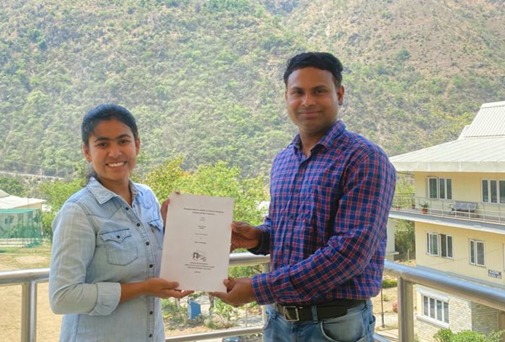
The findings of this study were published in the ACS Applied Materials Interfaces. The study was led by Dr. Viswanath Balakrishnan and co-authored by his student Ms. Divya Verma, Mr. Pawan Kumar & Ms Deepa Thakur. At the same time, density functional theory (DFT) simulations were done in collaboration with Prof. Chandra Singh, University of Toronto and Dr. Sankha Mukherjee, IIT Kharagpur. The project was funded by MHRD-STARS, India and Natural Sciences and Engineering Research Council of Canada (NSERC).
Atomically thin WS2 monolayers are widely known because of its direct bandgap, high mobility values and ability to provide a platform for heterogeneous integration of multiple functionalities. But the device fabrication of 2D materials using these monolayers is limited due to the lack of large-scale, crack-free growth of monolayers. However, IIT Mandi researchers have demonstrated that crack generation can be avoided despite defects and voids in a WS2 monolayer if CVD growth is performed on a suitable substrate such as sapphire.
Highlighting this research, Dr. Viswanath Balakrishnan, Associate Professor, School of Engineering, IIT Mandi, said, “Our team has carried out a systematic investigation to describe severe cracking in WS2 monolayer grown on different substrates by relating the thermal mismatch stress, substrate-monolayer binding energy, and the presence of defect-mediated voids formation.
Further, Dr. Viswanath Balakrishnan, said, “We have demonstrated that the crack generation can be avoided in spite of defects and voids in a WS2 monolayer, if CVD growth is performed on a suitable substrate and reported that the WS2 monolayer grown on sapphire substrate consisted of voids without any visible crack as it develops compressive residual stress in the WS2 monolayer.”
The growth of WS2 is also crucial as the growth temperature, growth substrate, and defect formation influence its mechanical stability. Substrate imposes residual stress during growth, and the effect may change because the thermal expansion coefficient will vary for different materials. So, to achieve a crack-free monolayer, one needs to optimize the thermal mismatch stress and the binding energy between the substrate and the monolayer.
Explaining the research, Ms. Divya Verma, research scholar, IIT Mandi, said, “WS2 monolayer grown on sapphire substrate can have voids or defects, yet it will not fracture as it develops compressive residual stress in the WS2 monolayer. This will be crucial for large scale crack free growth of WS2 monolayer where defect engineering is possible to enhance functionalities without the compromise in mechanical reliability.”
The team’s focus is mainly to develop CVD processed large scale 2D materials and demonstrate transistor, memristor and photodetector functions. However, prototyping such devices and proceeding towards heterogeneous integration will be done in collaboration with the experts from other IITs, IISc Bangalore in near future.

