
Researchers at IIT Roorkee are able to record Ultrafast photoresponse in SIS heterojunction-based NIR photodetectors
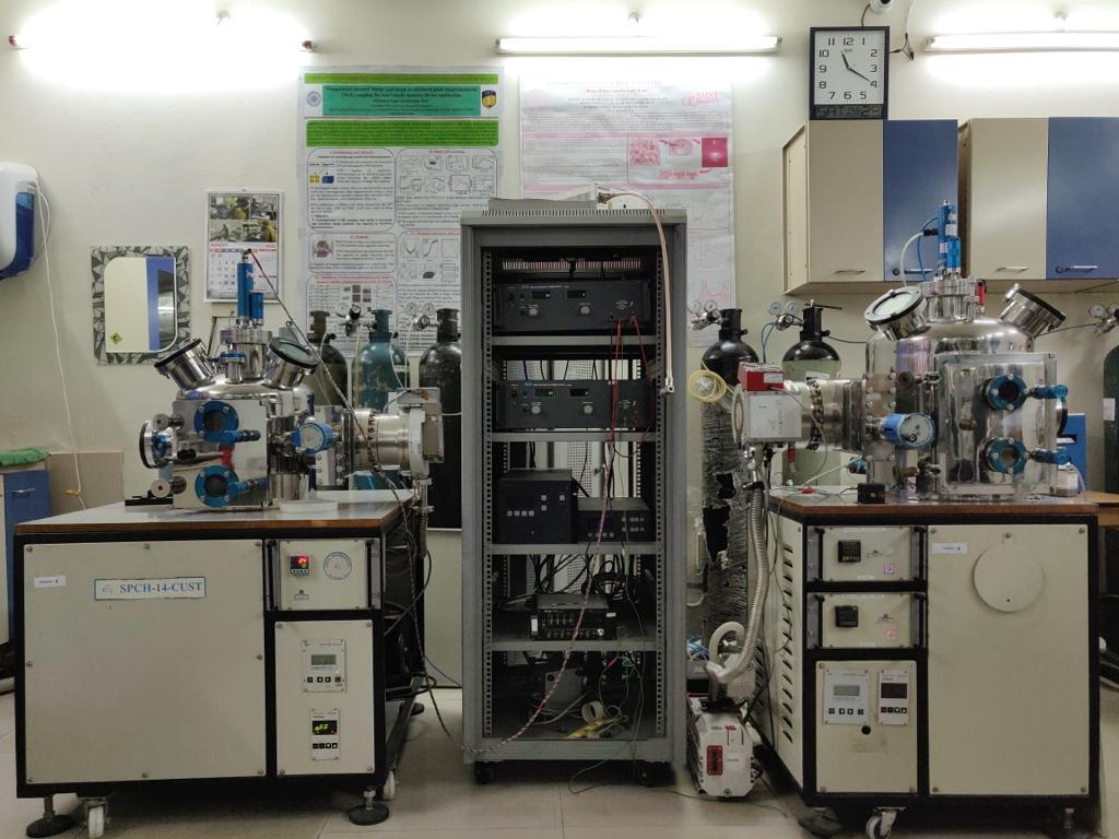
Roorkee : A team of researchers at the Indian Institute of Technology Roorkee (IIT Roorkee) led by Prof. Davinder Kaur, Dept of Physics, IIT Roorkee, along with the National Physical Laboratory, India, have been able to fabricate two Semiconductor-Insulator-Semiconductor (SIS) heterojunctions based Near-infrared (NIR) photodetectors for Ultrafast photoresponse by direct current (dc) magnetron sputtering technique. The DC magnetron sputtering process involves a vacuum chamber containing the target material parallel to the target substrate. The vacuum chamber contains a high-purity inert gas such as argon that becomes charged when exposed to a pulsed DC current.
The results demonstrate that SIS heterojunctions with an excellent carrier transport mechanism are potential candidates in next-generation ultrafast optoelectronics applications. The response time for both SIS n-MoS2/p-Si and n-MoS2/AlN/p-Si heterojunctions are found to be 0.3378 AW-1 and 1.865 AW-1 for visible radiations (532 nm) and 0.1245 AW-1 and 1.4743 AW-1 for NIR radiations (1064 nm), respectively. The response time (rise time and decay time) of the fabricated heterojunction decreased from 47.30 μs and 56.58 μs to 3.32 μs and 4.73 μs with the insertion of an ultrathin insulating AIN layer (plasma enhanced layer). This effort is a step before the new age of SIS heterostructure-based ultrafast-photovoltaic devices with the foremost carrier-tunnelling mechanism.
Numerous photodetectors have been developed with a significant photoresponse and using inorganic, organic and perovskite materials such as Silicon (Si), Gallium arsenide (GaAs), Zinc Oxide (ZnO), among others. Most of these photodetectors have certain limitations, such as relatively slow or less detection range or complicated and harmful techniques have been employed for the fabrication. Over the last decades, two-dimensional (2D) materials-based photodetectors have been in demand due to their low cost, miniature size, high sensitivity, and large available surface area for detection. In recent times, researchers have been interested in 2D materials and Si/GaAs-based heterojunction devices due to their ultrafast response, lightweight, and cost-effectiveness. In such heterojunction-based devices, 2D semiconducting materials help in device miniature with fast carrier transport and the ordinary semiconductors can absorb the maximum part of the incident light. However, MoS2/Si and MoS2/GaAs hybrid-heterojunction-based photonic devices were fabricated, but the semiconductor-insulator-semiconductor (SIS) heterojunctions of 2D MoS2 thin films had not been explored.
The research paper is named Solar Energy Materials and Solar Cells and has been published in ScienceDirect. You can visit the link to read the paper (www.elsevier.com/locate/solmat)
Krishan Kumar, Dept of Physics, IIT Roorkee, highlighted, “The photodetection parameters such as photocurrent, responsivity and response time have improved with the insertion of the insulating AIN layer. These results demonstrate that the heterostructure provides excellent opportunities for ultrafast photodetection application.”
Prof. K K Pant, Director IIT Roorkee, said, “Near-infrared photodetectors are a widespread and fundamental technology in many disciplines, from astronomy and telecommunications to medical sciences. This study proves functional and reliable to satisfy the new demands for wearable, cheap and flexible devices.”
Commenting on the importance of Ultrafast photoresponse in SIS heterojunction, Prof. Davinder Kaur, Dept. of Physics, IIT Roorkee, said, “The study will pave the way for cost-effective, highly sensitive, and ultrafast photodetectors of significant interest for various applications in optical communication, imaging, military operations, metrology, and monitoring ecological events. Moreover, the underline current conduction mechanism in SIS heterostructure-based photodetectors could be more exciting and make them robust for futuristic photodetectors applications.”