
Ural Federal University Experts Develop Effective Silicon Surface Processing Technology
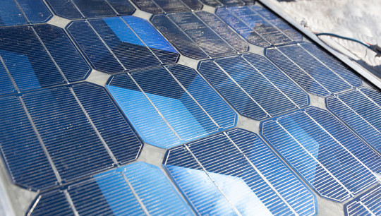
A team of scientists from Ekaterinburg (UrFU), Moscow, and St. Petersburg has developed a new technology for processing silicon wafers. It is a hybrid chemical and laser texturing, in which the wafer is treated with a femtosecond laser beam after chemical exposure to various reagents. Pre-chemical etching allows for five times faster laser treatment and improves light absorption over a broad spectral range. The technology will be useful in making solar cells. It could also be used in biomedicine for highly sensitive sensors for DNA analysis and detection of viruses and bacteria. It is also used in chemistry and in information and communication technologies. A description of the new technology has been published in the journal Materials.
“Currently, the formation of light-absorbing micro-reliefs on the surface of silicon wafers is achieved by a chemical process that is relatively inexpensive and used on an industrial scale. However, after chemical treatment, the wafers have a significant reflection coefficient, which reduces the efficiency of solar cells. An alternative method is laser treatment of the wafers. It reduces the reflection, but requires a significant amount of time using a femtosecond laser. Our proposed laser treatment after chemical etching reduces the processing time by a factor of five. At the same time, the reflection coefficient of wafers processed by the hybrid method is 7-10% lower than after chemical treatment,” says Vladimir Shur, Director of the Ural Multiple Access Center “Modern Nanotechnologies” of the UrFU.
The scientists used the equipment of the Ural Multiple Access Center “Modern Nanotechnologies” of the UrFU. The research was carried out with the partial financial support of the Ministry of Higher Education and Science of the Russian Federation under the development program “Priority 2030”.